What is a Pcb Board and How Does it Work?
A Pcb Board, or printed circuit board, is a foundation for electronic components. It connects and supports these components in devices we use daily. Dr. Emily Zhang, a leading expert in electronics engineering, states, “The PCB board is the heartbeat of modern technology.” This emphasizes the crucial role of PCB boards in our tech-driven world.
Understanding PCB boards involves exploring their design, materials, and functions. Each layer serves a purpose, allowing electricity to flow between components seamlessly. Nonetheless, many overlook the complexity involved in creating these essential boards. Common misconceptions can lead to confusion about their capabilities and limitations.
As the industry evolves, so too does the technology behind PCB boards. Emerging trends, such as flexible circuits, challenge traditional designs. Despite these advancements, some long-standing issues persist, like manufacturing inconsistencies and sustainability concerns. Reflecting on these challenges can inspire deeper discussions about the future of PCB boards and their impact on technology.
What is a PCB Board? Definition and Overview
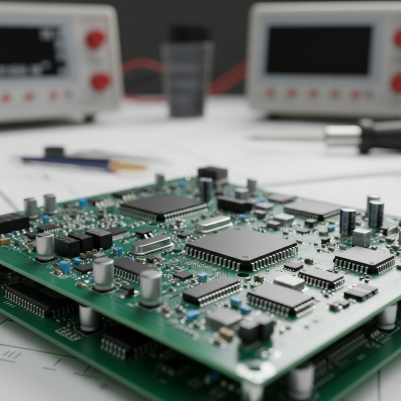
A PCB board, or printed circuit board, is crucial in electronics. It acts as the backbone of electronic devices. A typical PCB consists of a non-conductive substrate. This substrate is usually made from materials like fiberglass or epoxy resin. On this base, conductive pathways, made of copper, are etched. These pathways connect various electronic components, allowing them to communicate and function effectively.
The global PCB market has seen significant growth. According to a recent report from the IPC, the PCB industry is expected to reach $78.75 billion by 2025. This growth is driven by the increasing demand for consumer electronics, automotive systems, and healthcare devices. As technology evolves, PCBs are becoming more complex and compact. This complexity poses challenges in design and manufacturing. Sustainable practices are becoming essential. Many manufacturers are now exploring eco-friendly materials to reduce waste and environmental impact.
Understanding the design and functionality of PCB boards is vital. Each layer in a multi-layer PCB must be carefully planned. Errors can lead to failures in the final product. The balance between miniaturization and performance is a continuous challenge for engineers. Testing processes must be rigorous, as any oversight can be costly. The evolution of PCBs will likely continue to shape modern electronics.
Components of a PCB Board: A Breakdown of Elements
A PCB board, or printed circuit board, consists of various essential components that work together to ensure electronic devices function correctly. Understanding these components is crucial for anyone involved in electronics. The primary elements include the substrate, conductive pathways, and various electronic components.
The substrate serves as the base material, often made of fiberglass or epoxy resin. It provides structural integrity and insulation. Conductive pathways, typically copper traces, connect different components. These pathways deliver power and signals effectively across the board. This layout must be precise. Even minor mistakes can lead to circuit failure.
Components include resistors, capacitors, and integrated circuits. Each component plays a vital role. Resistors control current flow, while capacitors store energy. Integrated circuits can perform complex tasks.
**Tip: Always double-check connections on a PCB. A single misplaced component can disrupt the entire system.** Proper soldering technique enhances performance and longevity.
Designing a PCB requires attention to detail. It's easy to overlook small mistakes, like incorrect pad sizes. These can lead to functional issues later on.
**Tip: Use simulation software when designing. It helps avoid errors before production.** Testing prototype boards thoroughly is critical. It ensures that every component operates as intended.
Manufacturing Process of PCB Boards: Steps Involved
The manufacturing process of PCB boards involves several critical steps that ensure functionality and reliability. It begins with designing the PCB layout. Engineers utilize software tools to map out the circuitry precisely. This stage requires a keen eye for detail. Small mistakes can lead to significant issues later.
Once the design is validated, the next step is material selection. Typically, fiberglass or epoxy resin is used. The chosen materials must meet specific standards to ensure durability.
Afterward, the boards are printed with copper patterns. This is achieved through etching, where excess copper is removed. A steady hand is essential during this phase, as precision is key.
Tips: Always double-check your design files. Errors are easy to overlook. Review material specifications carefully to avoid compatibility issues.
After etching, the boards are drilled for component placements. This requires specialized machinery to create accurate holes. Following drilling, another layer of copper is applied. This builds up the circuit connections.
In the final stages, PCBs undergo testing for electrical integrity. Any faults must be identified and addressed before the boards are used. Despite advances in technology, human error can still occur. Regular training can minimize these risks. Understanding each step can enhance production efficiency and quality.
Functionality of PCB Boards: How They Operate in Electronics
Printed Circuit Boards (PCBs) are essential in modern electronics. They provide a platform for connecting electronic components. Their functionality relies on a combination of materials and design techniques. PCBs conduct electricity through conductive pathways, primarily made from copper. Insulation materials, such as FR-4, help to prevent short circuits between components.
The current market for PCB manufacturing is on the rise, with the industry valued at approximately $70 billion in 2022. Many reports predict a compound annual growth rate (CAGR) of about 7% over the next five years. This growth is driven by advancements in consumer electronics, automotive technology, and telecommunications. Efficient design and manufacturing processes contribute to a decrease in production costs, which also boosts accessibility for smaller companies.
Despite their advantages, PCBs are not without challenges. Designing a PCB requires precision. A minor error in the schematic can lead to significant functional issues. Additionally, the increasing complexity of devices necessitates further research. Engineers continually face the challenge of optimizing space on PCBs, especially as electronic components become smaller and more powerful. These ongoing issues highlight the need for innovation within the industry.
Applications of PCB Boards: Common Uses in Various Industries
PCB boards are essential in numerous industries. They serve as the backbone for electronic devices. Without them, many gadgets wouldn't function. Their applications range from consumer electronics to automotive systems.
In consumer electronics, PCBs connect components in smartphones and tablets. They help transmit signals effectively. In medical devices, PCBs are vital for monitoring systems. They ensure accurate readings in life-saving equipment. Moreover, automotive industries utilize PCBs for control systems and navigation. This enhances vehicle safety and efficiency.
Despite their importance, not all PCBs are created equally. Some might lack the durability needed for harsh environments. This can lead to failures in critical applications. It's vital to choose the right type for each use case. Reflecting on these factors can help improve functionality and reliability.
